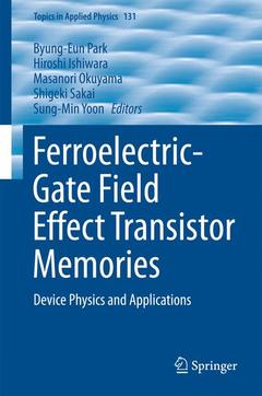
Ferroelectric-Gate Field Effect Transistor Memories, Softcover reprint of the original 1st ed. 2016 Device Physics and Applications Topics in Applied Physics Series, Vol. 131
Coordonnateurs : Park Byung-Eun, Ishiwara Hiroshi, Okuyama Masanori, Sakai Shigeki, Yoon Sung-Min

This book provides comprehensive coverage of the materials characteristics, process technologies, and device operations for memory field-effect transistors employing inorganic or organic ferroelectric thin films. This transistor-type ferroelectric memory has interesting fundamental device physics and potentially large industrial impact.
Among the various applications of ferroelectric thin films, the development of nonvolatile ferroelectric random access memory (FeRAM) has progressed most actively since the late 1980s and has achieved modest mass production levels for specific applications since 1995. There are two types of memory cells in ferroelectric nonvolatile memories. One is the capacitor-type FeRAM and the other is the field-effect transistor (FET)-type FeRAM. Although the FET-type FeRAM claims ultimate scalability and nondestructive readout characteristics, the capacitor-type FeRAMs have been the main interest for the major semiconductor memory companies, because the ferroelectric FET has fatal handicaps of cross-talk for random accessibility and short retention time.
This book aims to provide readers with the development history, technical issues, fabrication methodologies, and promising applications of FET-type ferroelectric memory devices, presenting a comprehensive review of past, present, and future technologies. The topics discussed will lead to further advances in large-area electronics implemented on glass or plastic substrates as well as in conventional Si electronics.
The book is composed of chapters written by leading researchers in ferroelectric materials and related device technologies, including oxide and organic ferroelectric thin films.
Preface
I. Operation Principle of One-Transistor Type Ferroelectric-gate Field Effect Transistors
II. Practical Characteristics of Inorganic Ferroelectric-gate FETs
Si-Based Ferroelectric-gate Field Effect Transistors
1) Pt/SrBi2Ta2O9(SBT)/(Hf,SiO)2/Si gate structure Ferroelectric FETs
2) Pt/(SBT,BLT)/HfO2/Si gate structure Ferroelectric FETs
Thin film-Based Ferroelectric-gate Field Effect Transistors
3) ITO/PZT/LaNiO3(LNO) gate structure Ferroelectric FETs
4) ZnO/Pb(Zr,Ti)O3 gate structure Ferroelectric FETs
5) Pt/PZT/ZnO gate structure Ferroelectric FETs
III. Practical Characteristics of Organic Ferroelectric-gate FETs
Si-Based Ferroelectric-gate Field Effect Transistors
1) Polyvinylidene fluoride (PVDF)/Si structure Ferroelectric-gate FETs
2) Poly(vinylidene fluoride-trifluoroethylene) (P(VDF-TrFE))/Si structure Ferroelectric-gate FETs
Thin film-Based Ferroelectric-gate Field Effect Transistors
3) P(VDF-TrFE)/Pentacene structure Ferroelectric-gate FETs
4) P(VDF-TrFE)/oxide thin film structure Ferroelectric-gate FETs
Ferroelectric-gate Field Effect Transistors with flexible substrates
5) P(VDF-TrFE)-based Ferroelectric-gate FETs fabricated on plastic substrates
6) P(VDF-TrFE)-based Ferroelectric-gate FETs fabricated on paper substrates
IV. Applications and Future Prospects
1) Novel Applications to NAND-type Memory Circuits
2) Novel Applications to Non-memory Devices
3) Features of One-Transistor Type Ferroelectric-gate Field Effect Transistors
Byung-Eun Park received the B.S. and M.S. degrees from the University of Seoul, Korea, and the Ph.D. degree in applied engineering from the Tokyo Institute of Technology, Tokyo, Japan.
He is a professor at School of Electrical and Computer Engineering, University of Seoul, Korea. Prior to joining the University of Seoul in 2004, he was an assistant professor in Tokyo Institute of Technology, and had joined the R&D Association for Future Electron Devices, Japan. He has over 250 patents including pending. Now, he is a non-executive director of Korea Intellectual Property Strategy Institute and a member of Compensation Council for duty invention of Seoul Metropolitan Government. His research interests are device and process technologies in ferroelectric memories. He also interests display devices, solar cells and sensors.
Hiroshi Ishiwara was born in Japan in 1945. He received the B.S., M.S., and Ph.D. degrees in electronic engineering from Tokyo Institute of Technology, Tokyo, Japan, in 1968, 1970, and 1973, respectively.
He was with the Tokyo Institute of Technology, as Research Associate (1973-1976), Associate Professor (1976-1989), and Professor (1989-2011). In 2004 and 2005, he was the Dean of professor at Interdisciplinary Graduate School of Science and Engineering. He retired from Tokyo Institute of Technology in 2011 and he is now a Professor Emeritus. In the period from 2010 to 2013, he was a WCU (World Class University) Professor in Department of Physics, Konkuk University, Korea. His research interests are device and process technologies in integrated circuits, particularly in ferroelectric memories. He has published 450 peer-reviewed papers with total citations more than 6000.
Dr. Ishiwara was awarded the Japan IBM Science Prize in 1990, International Symposium on Integrated Ferroelectrics 2000 Honors, the Purple Ribbon Medal by Japanese Government in 2003, Certificate of Merit in Nano Research Innovation Categ
Describes the development history, materials, fabrication methodologies, technical challenges and promising applications of FET-type ferroelectric memory devices
Presents a comprehensive review of past, present, and future technologies for the FET-type ferroelectric memories
Offers a useful source of information for graduate students of material science and electronic engineering, and device and process engineers in industry
Includes supplementary material: sn.pub/extras
Date de parution : 06-2018
Ouvrage de 347 p.
15.5x23.5 cm
Disponible chez l'éditeur (délai d'approvisionnement : 15 jours).
Prix indicatif 121,31 €
Ajouter au panierThème de Ferroelectric-Gate Field Effect Transistor Memories :
Mots-clés :
Ferroelectric-gate Field Effect Transistors; Field Effect Transistors with flexible; Inorganic Ferroelectric-gate FETs; NAND-type Memory Circuits; Non-memory Devices; One-Transistor Type; Organic Ferroelectric-gate FETs; Si-Based Ferroelectric-gate FETs; Thin film-Based Ferroelectric-gate FETs


