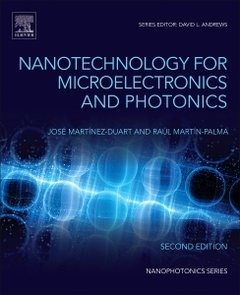
Nanotechnology for Microelectronics and Photonics (2nd Ed.) Nanophotonics Series
Auteurs : Martín-Palma Raúl José, Martínez-Duart José

Nanotechnology for Microelectronics and Photonics, Second Edition has been thoroughly revised, expanded, and updated. The aim of the book is to present the most recent advances in the field of nanomaterials, as well as the devices being developed for novel nanoelectronics and nanophotonic systems. It covers the many novel nanoscale applications in microelectronics and photonics that have been developed in recent years. Looking to the future, the book suggests what other applications are currently in development and may become feasible within the next few decades based on novel materials such as graphene, nanotubes, and organic semiconductors.
In addition, the inclusion of new chapters and new sections to keep up with the latest developments in this rapidly-evolving field makes Nanotechnology for Microelectronics and Photonics, Second Edition an invaluable reference to research and industrial scientists looking for a guide on how nanostructured materials and nanoscale devices are used in microelectronics, optoelectronics, and photonics today and in future developments.
José Martínez-Duart is Professor of Physics at Universidad Autónoma de Madrid, Spain. He is the author about three hundred publications in peer-reviewed scientific journals. During the 70s, he was Assistant Professor at Penn State University and Rensselaer Polytechnic Institute, and Research Visiting Scientist at the IBM T.J. Watson Research Center. Later was the Director of the Solid State Physics Institute (CSIC) at Madrid, and the Applied Physics Department at Universidad Autónoma, Madrid.
He is the former President of the European Materials Research Society (EMRS), 2000-1, and the first President of the Spanish Materials Society. During the last twenty years he has been working on the electronic and optoelectronic properties of nanostructured materials. His previous books several books with Elsevier, serving as Co-Editor of the two-volumes, “Materials and Processes for Submicron Technologies and “Current Trends in Nanotechnologies, as well as the first edition of the current book.
- Presents the fundamental scientific principles that explain the novel properties and applications of nanostructured materials in the quantum frontier
- Offers clear and concise coverage of how nanotechnology is currently used in the areas of microelectronics, optoelectronics, and photonics, as well as future proposed devices
- Includes nearly a hundred problems along with helpful hints and full solutions for more than half of them
Date de parution : 06-2017
Ouvrage de 336 p.
19x23.3 cm
Thèmes de Nanotechnology for Microelectronics and Photonics :
Mots-clés :
Absorption coefficient; Acceptor; Aharonov-Bohm effect; Artificial atom; Avalanche photodetector; Ballistic electron; Ballistic regime; Band structure; Bandtail states; Beyond CMOS; Beyond-CMOS devices; Bioelectronics; Bloch oscillations; Bloch oscillators; Bloch's theorem; CMOS; Composite fermion; Coulomb blockade; Coulomb island; Coupled quantum well (CQW)Heterojunction; Crystal momentum; Density of states; Devices for CMOS extension; Diffusive regime; Distribution function; DNA electronics; Edge states; Electroabsorption modulator; Flash memory; Fractional quantum Hall effect; Fullerene; Graphene; Hamiltonian operator; Heisenberg uncertainty principle; Heterostructure semiconductor laser; Hot electron; Index-guided laser; Interband transition; Landau level; Landauer-Buttiker formula; Law of mass action; Luminescence yield; Magnetic tunneling junction (MTJ)Metal base transistor (MBT)Negative differential resistance (NDR)Optoelectronic integrated circuit; Mean free path; Memristor; Moore's law; MOSFET; Multiple quantum well (MQW)nipi superlattice; Nanophotonics; Negative differential resistance; Population inversion; Quantum dot; Quantum well (QW)Superlattice (SL)Quantum-confined; Rydberg constant; Schrödinger equation; Selection rules; Self-assembled quantum dot; Silicene; Solar cell; Spintronics; Square potential well; Standard of resistance; Stanene; Stark effect; Stark ladder; Stark ladders; Stripe geometry configuration; Strong confinement regime; Therapy; Top-down nanofabrication; Triangular potential well; Tunnel magnetoresistance (TMR) effect; Velocity-overshoot effect; Vertical-cavity surface-emitting laser (VCSEL; Wannier-Mott exciton; Wave function; Weak confinement regime; Wigner crystal


