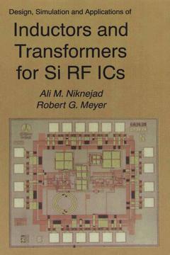
Design, Simulation and Applications of Inductors and Transformers for Si RF ICs, Softcover reprint of the original 1st ed. 2000 The Springer International Series in Engineering and Computer Science Series, Vol. 586
Langue : Anglais
Auteurs : Niknejad Ali M., Meyer Robert G.

The modern wireless communication industry has put great demands on circuit designers for smaller, cheaper transceivers in the gigahertz frequency range. One tool which has assisted designers in satisfying these requirements is the use of on-chip inductiveelements (inductors and transformers) in silicon (Si) radio-frequency (RF) integrated circuits (ICs). These elements allow greatly improved levels of performance in Si monolithic low-noise amplifiers, power amplifiers, up-conversion and down-conversion mixers and local oscillators. Inductors can be used to improve the intermodulation distortion performance and noise figure of small-signal amplifiers and mixers. In addition, the gain of amplifier stages can be enhanced and the realization of low-cost on-chip local oscillators with good phase noise characteristics is made feasible. In order to reap these benefits, it is essential that the IC designer be able to predict and optimize the characteristics of on-chip inductiveelements. Accurate knowledge of inductance values, quality factor (Q) and the influence of ad- cent elements (on-chip proximity effects) and substrate losses is essential. In this book the analysis, modeling and application of on-chip inductive elements is considered. Using analyses based on Maxwells equations, an accurate and efficient technique is developed to model these elements over a wide frequency range. Energy loss to the conductive substrate is modeled through several mechanisms, including electrically induced displacement and conductive c- rents and by magnetically induced eddy currents. These techniques have been compiled in a user-friendly software tool ASITIC (Analysis and Simulation of Inductors and Transformers for Integrated Circuits).
List of Figures. List of Tables. Preface. Acknowledgments. Part I: Analysis and Simulation of Passive Devices. 1. Introduction. 2. Problem Description. 3. Previous Work. 4. Electromagnetic Formulation. 5. Inductance Calculations. 6. Calculation of Eddy Current Losses. 7. Asitic. 8. Experimental Study. Part II: Applications of Passive Devices. 9. Voltage Controlled Oscillators. 10. Distributed Amplifiers. 11. Conclusion. Appendices.
Date de parution : 03-2013
Ouvrage de 190 p.
15.5x23.5 cm
Disponible chez l'éditeur (délai d'approvisionnement : 15 jours).
Prix indicatif 189,89 €
Ajouter au panierDate de parution : 10-2000
Ouvrage de 190 p.
15.6x23.4 cm
Thème de Design, Simulation and Applications of Inductors and... :
© 2024 LAVOISIER S.A.S.
