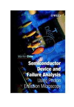
Semiconductor Device and Failure Analysis Using Photon Emission Microscopy
Auteur : Chim Wai Kin

* Illustrates the application of the PEM technique in various areas of device reliability, in particular hot-carrier, oxide and ESD reliability.
* Presents the principles of design and calibration for a spectroscopic emission microscope system along with coverage of the three main operation modes: frontside, backside and spectroscopic PEM
* Provides an analysis of light emission in semiconductors under hot-carrier and high-field impulse stressing in MOS transistors and photon emission from biased MOS capacitors.
Not only an essential reference for researchers and students in the field, the numerous practical examples throughout the text also make this an indispensible guide for failure analysis engineers and microelectrics industry professionals.
Introduction.
Theory of Light Emission in Semiconductors.
Instrumentation Aspects of the Photon Emission Microscope.
Backside Photon Emission Microscopy.
Spectroscopic Photon Emission Microscopy.
Photon Emission from Metal-Oxide-Semiconductor Field-Effect Transistors under Hot-Carrier Stressing.
Photon Emission from Metal-Oxide-Semiconductor Field-Effect Transistors under High-Field Impulse Stressing.
Oxide Degradation and Photon Emission from Metal-Oxide Semiconductor Capacitor Structures.
Index.
Wai Kin Chim is the author of Semiconductor Device and Failure Analysis : Using Photon Emission Microscopy , published by Wiley.
Date de parution : 12-2000
Ouvrage de 288 p.
16x23.7 cm
Thème de Semiconductor Device and Failure Analysis :
Mots-clés :
detection; greater; integrated circuits; modern; diminishing; fault; semiconductor; new challenges; analysing ic; physical; photon; microscopy; localisation; pem; failures; emission; technique; application; device; areas
