Lavoisier S.A.S.
14 rue de Provigny
94236 Cachan cedex
FRANCE

Heures d'ouverture 08h30-12h30/13h30-17h30
Tél.: +33 (0)1 47 40 67 00
Fax: +33 (0)1 47 40 67 02


Url canonique : www.lavoisier.fr/livre/physique/engineering-thin-films-et-nanostructures-with-ion-beams-with-cd-rom/knystautas/descriptif_1664959
Url courte ou permalien : www.lavoisier.fr/livre/notice.asp?ouvrage=1664959

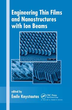
Engineering Thin Films and Nanostructures with Ion Beams

Langue : Anglais

Coordonnateur : Knystautas Emile

Couverture de l’ouvrage Engineering Thin Films and Nanostructures with Ion Beams

While ion-beam techniques have been used to create thin films in the semiconductor industry for several decades, these methods have been too costly for other surface treatment applications. However, as manufacturing devices become increasingly smaller, the use of a directed-energy ion beam is finding novel industrial applications that require the custom tailoring of new materials and devices, including magnetic storage devices, photonics, opto-electronics, and molecular transport. Engineering Thin Films and Nanostructures with Ion Beams offers a thorough narrative of the recent advances that make this technology relevant to current and future applications.

Featuring internationally recognized researchers, the book compiles their expertise in a multidimensional source that:

  • Highlights the mechanisms and visual evidence of the effects of single-ion impacts on metallic surfaces
  • Considers how ion-beam techniques can help achieve higher disk-drive densities
  • Introduces gas-cluster ion-beam technology and reviews its precedents
  • Explains how ion beams are used to aggregate metals and semiconductors into nanoclusters with nonlinear optical properties
  • Addresses current challenges in building equipment needed to produce nanostructures in an industrial setting
  • Examines the combination of ion-beam techniques, particularly with physical vapor deposition
  • Delineates the fabrication of nanopillars, nanoflowers, and interconnected nanochannels in three dimensions by using atomic shadowing techniques
  • Illustrates the production of nanopores of varying dimensions in polymer films, alloys, and superconductors using ion-beam irradiation
  • Shows how fingerprints can be made more reliable as forensic evidence by recoil-mixing them into the substrate using ion beams

    From the basics of the ion-beam modification of materials to state-of-the-art applications, Engineering Th
  • Introduction, Single Ion Induced Spike Effects on Thin Metal Films: Observation and Simulation, on Beam Effects in Magnetic Thin Films, Selected Topics in Ion Beam Surface Engineering, Optical Effects of Ion Implantation, Metal Alloy Nanoclusters by Ion Implantation in Silica, Intrinsic Residual Stress Evolution in Thin Films During Energetic Particle Bombardment, Industrial Aspects of Ion Implantation Equipment and Ion Beam Generation, Nanostructured Transition-Metal Layers, Nuclear Tracks and Nanostructures, Forensic Applications of Ion-Beam Mixing and Surface Spectroscopy of Latent Fingerprints, Glossary
    Academic and Professional Practice & Development
    Émile Knystautas

    Date de parution :

    15.2x22.9 cm

    Disponible chez l'éditeur (délai d'approvisionnement : 14 jours).

    77,28 €

    Ajouter au panier

    Date de parution :

    Ouvrage de 400 p.

    15.2x22.9 cm

    Sous réserve de disponibilité chez l'éditeur.

    324,90 €

    Ajouter au panier