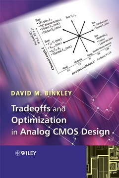
Tradeoffs and Optimization in Analog CMOS Design
Auteur : Binkley David

This book addresses tradeoffs and optimization of device and circuit performance for selections of the drain current, inversion coefficient, and channel length, where channel width is implicitly considered. The inversion coefficient is used as a technology independent measure of MOS inversion that permits design freely in weak, moderate, and strong inversion.
This book details the significant performance tradeoffs available in analog CMOS design and guides the designer towards optimum design by describing:
- An interpretation of MOS modeling for the analog designer, motivated by the EKV MOS model, using tabulated hand expressions and figures that give performance and tradeoffs for the design choices of drain current, inversion coefficient, and channel length; performance includes effective gate-source bias and drain-source saturation voltages, transconductance efficiency, transconductance distortion, normalized drain-source conductance, capacitances, gain and bandwidth measures, thermal and flicker noise, mismatch, and gate and drain leakage current
- Measured data that validates the inclusion of important small-geometry effects like velocity saturation, vertical-field mobility reduction, drain-induced barrier lowering, and inversion-level increases in gate-referred, flicker noise voltage
- In-depth treatment of moderate inversion, which offers low bias compliance voltages, high transconductance efficiency, and good immunity to velocity saturation effects for circuits designed in modern, low-voltage processes
- Fabricated design examples that include operational transconductance amplifiers optimized for various tradeoffs in DC and AC performance, and micropower, low-noise preamplifiers optimized for minimum thermal and flicker noise
- A design spreadsheet, available at the book web site, that facilitates rapid, optimum design of MOS devices and circuits
Tradeoffs and Optimization in Analog CMOS Design is the first book dedicated to this important topic. It will help practicing analog circuit designers and advanced students of electrical engineering build design intuition, rapidly optimize circuit performance during initial design, and minimize trial-and-error circuit simulations.
Preface.
Acknowledgments.
List of Symbols and Abbreviations.
1 Introduction.
1.1 Importance of Tradeoffs and Optimization in Analog CMOS Design.
1.2 Industry Designers and University Students as Readers.
1.3 Organization and Overview of Book.
1.4 Full or Selective Reading of Book.
1.5 Example Technologies and Technology Extensions.
1.6 Limitations of the Methods.
1.7 Disclaimer.
PART I MOS Device Performance, Tradeoffs and Optimization for Analog CMOS Design.
2 MOS Design from Weak through Strong Inversion.
2.1 Introduction.
2.2 MOS Design Complexity Compared to Bipolar Design.
2.3 Bipolar Transistor Collector Current and Transconductance.
2.4 MOS Drain Current and Transconductance.
2.5 MOS Drain–Source Conductance.
2.6 Analog CMOS Electronic Design Automation Tools and Design Methods.
References.
3 MOS Performance versus Drain Current, Inversion Coefficient, and Channel Length.
3.1 Introduction.
3.2 Advantages of Selecting Drain Current, Inversion Coefficient, and Channel Length in Analog CMOS Design.
3.3 Process Parameters for Example Processes.
3.4 Substrate Factor and Inversion Coefficient.
3.5 Temperature Effects.
3.6 Sizing Relationships.
3.7 Drain Current and Bias Voltages.
3.8 Small-Signal Parameters and Intrinsic Voltage Gain.
3.9 Capacitances and Bandwidth.
3.10 Noise.
3.11 Mismatch.
3.12 Leakage Current.
References.
4 Tradeoffs in MOS Performance, and Design of Differential Pairs and Current Mirrors.
4.1 Introduction.
4.2 Performance Trends.
4.3 Performance Tradeoffs.
4.4 Design of Differential Pairs and Current Mirrors Using the Analog CMOS Design, Tradeoffs and Optimization Spreadsheet.
References.
PART II Circuit Design Examples Illustrating Optimization for Analog CMOS Design.
5 Design of CMOS Operational Transconductance Amplifiers Optimized for DC, Balanced, and AC Performance.
5.1 Introduction.
5.2 Circuit Description.
5.3 Circuit Analysis and Performance Optimization.
5.4 Design Optimization and Resulting Performance for the Simple OTAs.
5.5 Design Optimization and Resulting Performance for the Cascoded OTAs.
5.6 Prediction Accuracy for Design Guidance and Optimization.
References.
6 Design of Micropower CMOS Preamplifiers Optimized for Low Thermal and Flicker Noise.
6.1 Introduction.
6.2 Using the Lateral Bipolar Transistor for Low-Flicker-Noise Applications.
6.3 Measures of Preamplifier Noise Performance.
6.4 Reported Micropower, Low-Noise CMOS Preamplifiers.
6.5 MOS Noise versus the Bias Compliance Voltage.
6.6 Extraction of MOS Flicker-Noise Parameters.
6.7 Differential Input Preamplifier.
6.8 Single-Ended Input Preamplifier.
6.9 Prediction Accuracy for Design Guidance and Optimization.
6.10 Summary of Low-Noise Design Methods and Resulting Challenges in Low-Voltage Processes.
References.
7 Extending Optimization Methods to Smaller-Geometry CMOS Processes and Future Technologies.
7.1 Introduction.
7.2 Using the Inversion Coefficient for CMOS Process Independence and for Extension to Smaller-Geometry Processes.
7.3 Enhancing Optimization Methods by Including Gate Leakage Current Effects.
7.4 Using an Inversion Coefficient Measure for Non-CMOS Technologies.
References.
Appendix: The Analog CMOS Design, Tradeoffs and Optimization Spreadsheet.
Index.
David Binkley is currently Associate Professor in the Department of Electrical and Computer Engineering, at the University of North Carolina at Charlotte, a post he has held since 2000. He teaches a number of courses in analog, mixed-signal, and RF integrated circuit design, and received the Tau Beta Pi "Most Influential Teacher of 2001" award for the college of engineering. He has a wealth of experience in the field of analog and mixed signal engineering, having been a practising engineer for over 20 years and having co-founded Concorde Microsystems in 1992 where he and colleagues developed custom, mixed-signal CMOS (complementary metal-oxide-semiconductor) integrated circuits. Previous to this, he was a senior scientist at CTI/Siemens PET Systems engaged in research and design of circuits for PET medical imaging tomographs. David has also been the principal investigator on a number of research projects receiving support from NASA JPL for micropower, analog CMOS circuits, and DARPA (Defense Advanced Research Projects Agency) for design and testing methodologies for mixed-signal integrated circuits. He has published over 60 papers and regularly gives short courses on optimizing analog CMOS design.
Date de parution : 08-2008
Ouvrage de 632 p.
17.7x25.1 cm
Thème de Tradeoffs and Optimization in Analog CMOS Design :
Mots-clés :
list; cmos design; tradeoffs; importance; analog; industry; readers; book; overview; reading; selective; methods; part; performance; design; cmos; mos design; strong inversion; complexity; bipolar; mos; compared; collector


