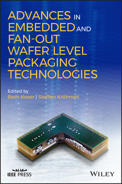
Advances in Embedded and Fan-Out Wafer Level Packaging Technologies IEEE Press Series
Coordonnateurs : Keser Beth, Kröhnert Steffen

Examines the advantages of Embedded and FO-WLP technologies, potential application spaces, package structures available in the industry, process flows, and material challenges
Embedded and fan-out wafer level packaging (FO-WLP) technologies have been developed across the industry over the past 15 years and have been in high volume manufacturing for nearly a decade. This book covers the advances that have been made in this new packaging technology and discusses the many benefits it provides to the electronic packaging industry and supply chain. It provides a compact overview of the major types of technologies offered in this field, on what is available, how it is processed, what is driving its development, and the pros and cons.
Filled with contributions from some of the field's leading experts,Advances in Embedded and Fan-Out Wafer Level Packaging Technologies begins with a look at the history of the technology. It then goes on to examine the biggest technology and marketing trends. Other sections are dedicated to chip-first FO-WLP, chip-last FO-WLP, embedded die packaging, materials challenges, equipment challenges, and resulting technology fusions.
- Discusses specific company standards and their development results
- Content relates to practice as well as to contemporary and future challenges in electronics system integration and packaging
Advances in Embedded and Fan-Out Wafer Level Packaging Technologies will appeal to microelectronic packaging engineers, managers, and decision makers working in OEMs, IDMs, IFMs, OSATs, silicon foundries, materials suppliers, equipment suppliers, and CAD tool suppliers. It is also an excellent book for professors and graduate students working in microelectronic packaging research.
Preface xvii
List of Contributors xxiii
Acknowledgments xxvii
1 History of Embedded and Fan-Out Packaging Technology 1
Michael Topper, Andreas Ostmann, Tanja Braun, and Klaus-Dieter Lang
2 FO-WLP Market and Technology Trends 39
E. Jan Vardaman
3 Embedded Wafer-Level Ball Grid Array (eWLB) Packaging Technology Platform 55
Thorsten Meyer and Steffen Krohnert
4 Ultrathin 3D FO-WLP eWLB-PoP (Embedded Wafer-Level Ball Grid Array-Package-on-Package) Technology 77
S.W. Yoon
5 NEPES’ Fan-Out Packaging Technology from Single die, SiP to Panel-Level Packaging 97
Jong Heon (Jay) Kim
6 M-Series Fan-Out with Adaptive Patterning 117
Tim Olson and Chris Scanlan
7 SWIFTR Semiconductor Packaging Technology 141
Ron Huemoeller and Curtis Zwenger
8 Embedded Silicon Fan-Out (eSiFOR) Technology for Wafer-Level System Integration 169
Daquan Yu
9 Embedding of Active and Passive Devices by Using an Embedded Interposer: The i2 Board Technology 185
Thomas Gottwald, Christian Roessle, and Alexander Neumann
10 Embedding of Power Electronic Components: The Smart p2 Pack Technology 201
Thomas Gottwald and Christian Roessle
11 Embedded Die in Substrate (Panel-Level) Packaging Technology 217
Tomoko Takahashi and Akio Katsumata
12 Blade: A Chip-First Embedded Technology for Power Packaging 241
Boris Plikat and Thorsten Scharf
13 The Role of Liquid Molding Compounds in the Success of Fan-Out Wafer-Level Packaging Technology 261
Katsushi Kan, Michiyasu Sugahara, and Markus Cichon
14 Advanced Dielectric Materials (Polyimides and Polybenzoxazoles) for Fan-Out Wafer-Level Packaging (FO-WLP) 271
T. Enomoto, J.I. Matthews, and T. Motobe
15 Enabling Low Temperature Cure Dielectrics for Advanced Wafer-Level Packaging 317
Stefan Vanclooster and Dimitri Janssen
16 The Role of Pick and Place in Fan-Out Wafer-Level Packaging 347
Hugo Pristauz, Alastair Attard, and Harald Meixner
17 Process and Equipment for eWLB: Chip Embedding by Molding 371
Edward Furgut, Hirohito Oshimori, and Hiroaki Yamagishi
18 Tools for Fan-Out Wafer-Level Package Processing 403
Nelson Fan, Eric Kuah, Eric Ng, and Otto Cheung
19 Equipment and Process for eWLB: Required PVD/Sputter Solutions 419
Chris Jones, Ricardo Gaio, and Jose Castro
20 Excimer Laser Ablation for the Patterning of Ultra-fine Routings 441
Habib Hichri, Markus Arendt, and Seongkuk Lee
21 Temporary Carrier Technologies for eWLB and RDL-First Fan-Out Wafer-Level Packages 457
Thomas Uhrmann and Boris Povaay
22 Encapsulated Wafer-Level Package Technology (eWLCSP): Robust WLCSP Reliability with Sidewall Protection 471
S.W. Yoon
23 Embedded Multi-die Interconnect Bridge (EMIB): A Localized, High Density, High Bandwidth Packaging Interconnect 487
Ravi Mahajan, Robert Sankman, Kemal Aygun, Zhiguo Qian, Ashish Dhall, Jonathan Rosch, Debendra Mallik, and Islam Salama
24 Interconnection Technology Innovations in 2.5D Integrated Electronic Systems 501
Paragkumar A. Thadesar, Paul K. Jo, and Muhannad S. Bakir
References 515
Index 521
Beth Keser, Ph.D., is a recognized global leader in the semiconductor industry with over 20 years' experience resulting in 28 patents and patents pending and over 40 publications. She is an IEEE Senior Member whose volunteer activities and professional society responsibilities include: IEEE EPS' VP of Education, 2015 ECTC General Chair, and more.
Steffen Kröhnert, M.SC., is Senior Director of Technology Development at Amkor Technology Holding B.V., Germany. He has more than 20 years' experience in the semiconductor industry. Steffen is author and co-author of 23 patent filings in the area of Semiconductor Packaging Technology, and an active member of IEEE EPS, IMAPS, SMTA, VDI, VDE and GPM.
Date de parution : 02-2019
Ouvrage de 576 p.
15.8x23.4 cm
Thème d’Advances in Embedded and Fan-Out Wafer Level Packaging... :
Mots-clés :
embedded packaging; fan-out wafer level packaging; FO-WLP; electronic packaging; microelectronic packaging; guide to microelectronic packaging; guide to embedded technology; guide to FO-WLP; microelectronic packaging research; microelectronic packaging technology; FO-WLP technologies; embedded technologies; FO-WLP technology applications; embedded and fan-out wafer level packaging technologies package structure; embedded and fan-out wafer level packaging technologies process flows; electronic packaging material challenges; packaging technology; the electronic packaging industry; trends in the electronic packaging industry; FO-WLP trends; embedded wafer-level ball grid array packaging technology; eWLB packaging technology; device packaging; embedded and fan-out wafer level packaging technologies advances; Advances in Embedded and Fan-Out Wafer Level Packaging Technologies


