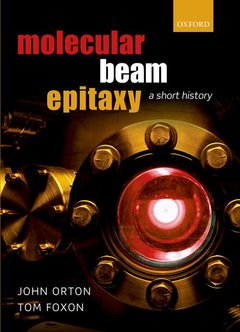
Molecular Beam Epitaxy A Short History
Langue : Anglais
Auteurs : Orton John, Foxon Tom

The book is a history of Molecular Beam Epitaxy (MBE) as applied to the growth of semiconductor thin films (note that it does not cover the subject of metal thin films). It begins by examining the origins of MBE, first of all looking at the nature of molecular beams and considering their application to fundamental physics, to the development of nuclear magnetic resonance and to the invention of the microwave MASER. It shows how molecular beams of silane (SiH4) were used to study the nucleation of silicon films on a silicon substrate and how such studies were extended to compound semiconductors such as GaAs. From such surface studies in ultra-high vacuum the technique developed into a method of growing high quality single crystal films of a wide range of semiconductors. Comparing this with earlier evaporation methods of deposition and with other epitaxial deposition methods such as liquid phase and vapour phase epitaxy (LPE and VPE). The text describes the development of MBE machines from the early âhome-madeâ variety to that of commercial equipment and show how MBE was gradually refined to produce high quality films with atomic dimensions. This was much aided by the use of various in-situ surface analysis techniques, such as reflection high energy electron diffraction (RHEED) and mass spectrometry, a feature unique to MBE. It looks at various modified versions of the basic MBE process, then proceed to describe their application to the growth of so-called âlow-dimensional structuresâ (LDS) based on ultra-thin heterostructure films with thickness of order a few molecular monolayers. Further chapters cover the growth of a wide range of different compounds and describe their application to fundamental physics and to the fabrication of electronic and opto-electronic devices. The authors study the historical development of all these aspects and emphasise both the (often unexpected) manner of their discovery and development and the unique features which MBE brings to the growth of extremely complex structures with monolayer accuracy.
John Orton won an Exhibition at Magdalen College, Oxford, where he obtained an honours degree in Physics, followed by a D Phil, with a thesis on Electron Spin Resonance in magnesium oxide. He joined Mullard (later Philips) Research Laboratories in 1960 to work on the development of the microwave maser. In 1968 he lead the Group responsible for developing compound semiconductor devices and continued to work in various aspects of semiconductor research, one of his principal interests being in the use of Molecular Beam Epitaxy to grow low-dimensional semiconductor structures. from 1989 to 1991 he was Visiting Professor in Nottingham. He was active within the Institute of Physics, serving on the Solid State Physics Committee, the Semiconductor Physics Committee and on the Editorial Board of J Phys D (Applied Physics). In 1991 he took up the Chair of Optoelectronics in the Department of Electrical and Electronic Engineering at the University of Nottingham. Tom Foxon obtained his B.Sc. in Physics at King's College, London and his Ph.D. in Materials Science in, at Battersea College. In 1969 he joined the Mullard (now Philips) Research Laboratories where he started the first work in Europe on MBE growth of III-V compounds. In 1987 he was appointed as a Visiting Professor in the Physics Department of the Technical University in Eindhoven, the Netherlands. In October 1991, he was appointed to his present post as a Professor in the School of Physics and Astronomy at the University of Nottingham, where in collaboration with Prof John Orton he set up the first work in Europe on the growth of group III-Nitride by MBE. He is currently Chairman of the UK Nitride Consortium, a member of the UK MBE group, a member of the EPSRC Peer Review College, a Fellow of the IOP, was President of the British Association for Crystal Growth (2006-2009) and was elected a Fellow of the Royal Society in 2006.
Date de parution : 06-2015
Ouvrage de 530 p.
19.3x25.9 cm
Thème de Molecular Beam Epitaxy :
© 2024 LAVOISIER S.A.S.
