Epitaxy of Semiconductors (2nd Ed., 2nd ed. 2020) Physics and Fabrication of Heterostructures Graduate Texts in Physics Series
Auteur : Pohl Udo W.
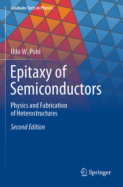
The extended and revised edition of this textbook provides essential information for a comprehensive upper-level graduate course on the crystalline growth of semiconductor heterostructures. Heteroepitaxy is the basis of today?s advanced electronic and optoelectronic devices, and it is considered one of the most important fields in materials research and nanotechnology. The book discusses the structural and electronic properties of strained epitaxial layers, the thermodynamics and kinetics of layer growth, and it describes the major growth techniques: metalorganic vapor-phase epitaxy, molecular-beam epitaxy, and liquid-phase epitaxy. It also examines in detail cubic and hexagonal semiconductors, strain relaxation by misfit dislocations, strain and confinement effects on electronic states, surface structures, and processes during nucleation and growth. Requiring only minimal knowledge of solid-state physics, it provides natural sciences, materials science and electrical engineering students and their lecturers elementary introductions to the theory and practice of epitaxial growth, supported by references and over 300 detailed illustrations. In this second edition, many topics have been extended and treated in more detail, e.g. in situ growth monitoring, application of surfactants, properties of dislocations and defects in organic crystals, and special growth techniques like vapor-liquid-solid growth of nanowires and selective-area epitaxy.
Dr. rer. nat. Udo W. Pohl, professor of experimental physics, studied physics in Aachen and Berlin, Germany, and received his Ph.D. degree in 1988 from the Technical University of Berlin, where he is currently principal investigator in the Institute of Solid State Physics. He is a member of the German Physical Society, participated in international conference committees, and has given keynote addresses at international conferences. Since the early 1990ies he has given lectures on semiconductor physics and epitaxy. In 2009, he was appointed Adjunct Professor of Physics at Technical University of Berlin. He is series editor of Materials Sciences, has authored over 200 journal articles and conference papers, the books Epitaxy of Semiconductors and – together with Prof. Dr. Karl W. Böer – Semiconductor Physics, thirteen book contributions, and patents. His current research interests include physics and epitaxy of semiconductor nanostructures and devices.
Provides the essentials for a comprehensive graduate course on crystal growth of semiconductor heterostructures
Covers thermodynamics and kinetics of layer growth and major growth techniques
Contains many instructive illustrations and examples
Supports learning with exercises after each chapter and solutions in the end of the book
Date de parution : 07-2021
Ouvrage de 535 p.
15.5x23.5 cm
Disponible chez l'éditeur (délai d'approvisionnement : 15 jours).
Prix indicatif 68,56 €
Ajouter au panierDate de parution : 07-2020
Ouvrage de 535 p.
15.5x23.5 cm